
By Chris Francis
There are a number of DDS chips around. Taking Analog Devices as an example, they range from simple, low speed, low cost devices such as the AD9837 (5MHz or 16MHz clock) for around $2 to the AD9914 3.5Gs/s costing over $180. Some are aimed at function generators, some for test and measurement, some for RF frequency applications. Typically their main function is generating sine waves with the main benefit that they can change frequency very quickly as they are based on a sine lookup table and DAC rather than a PLL, i.e. they are very frequency agile.
There are a number of cheap AD9850 boards available on the internet – costing less than half the price of the chip itself! While there are various theories for this, the most plausible is that they were built incorrectly – the filter is wrong. For the ones that include a circuit diagram, you will see a 70MHz Elliptic 7th order filter with component values straight from the AD9851 datasheet. However, the AD9851 runs at 180MHz and the AD9850 only runs at 125MHz so a 42MHz filter, as shown in the AD9850 datasheet is more appropriate. The boards are still usable – you will just get higher level spurious components unless you change the filter components.
Calculating the values for programming the chip is straightforward. There are a couple of design tools to help such as:
- http://designtools.analog.com/dt/dds/ad9850.html
- http://designtools.analog.com/dtDDSWeb/dtDDSMain.aspx
The first tool is handy in that it also shows the data for sending serially by SPI as well as by parallel interface. Parallel data is sent in 5 bytes with the most significant byte first. SPI data is sent as a 40 bit string with the least significant bit first. Often this will be using a microcontroller 8 bits at a time. However, a microcontroller will usually send the most significant bit (MSB) first so the bits in each byte also need reversing. So, if the parallel byte is 7A, the serial byte to be sent is 5E in order to get the bit order correct i.e. 01011110 instead of 01111010. Be sure to read the serial section carefully to get the chip in to serial mode, which involves setting D0 & D1 to logic 1 and D2 to logic 0 and clocking W_CLK before trying to send data.
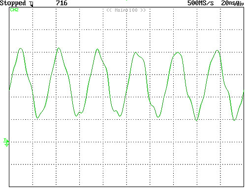
The quality of the output waveform is very dependent on the quality of the filtering when you approach half the sampling frequency. Even at 30MHz (with 125MHz sampling) the waveform is not great:
The waveform shown by the Analog Devices design tools looks a lot cleaner but that is using a theoretical filter rather than actual components. A spectrum analyzer trace of the output (using an active, low capacitance probe) is shown below:
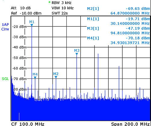
Some of the significant spurious signals are marked. There is also a second harmonic (60MHz) at -76dBm which is difficult to see as it falls over a grid line. These were with a 42MHz 5 pole Elliptical filter as in the AD9850 datasheet. These compare with the theoretical values as follows:
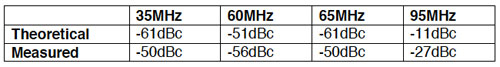
At 35MHz and 65MHz the spurious components are around 11dB worse than the theory which probably accounts for the worse looking waveform on an oscilloscope. This is probably to do with the quality of the components used in the filter as well as spurious effects such as inductor self resonant frequency (SRF) and Q. The Spurious at 60MHz and 95MHz are actually better than the theory! This is actually not difficult to understand when you look at the response of the 5 pole Elliptical filter used:
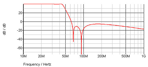
As luck would have it, 65MHz falls just where there is a notch in the Elliptical filter as does 95MHz! The exact notch positions are highly dependent on the actual component values and these simulations doe not take account of the SRF/Q so reality could be a little different. It does show how the filter can significantly affect the results. The Analog Devices calculator allows you to input the filter characteristics (e.g. 5 pole Elliptical with 42MHz cutoff) but it seems to assume a flat stop band attenuation ignoring the ripple. To get the best spurious response would require some careful selection of the filter components and the PCB layout, as well as possibly a modified filter design to suppress spurious frequencies if the operating frequency of interest is a narrow, known range.