When designing opamps in analog IC design, it is frequently required to plot the open loop gain/phase. One way of doing that is to use a high feedback resistor and very high capacitance so the feedback network has an extremely low corner frequency:

This works fine unless your opamp drive capability is low, in which case you can increase the feedback resistor. However, if the opamp also has a significant bias current that will shift the bias point of the opamp which could saturate the opamp output in extreme circumstances.
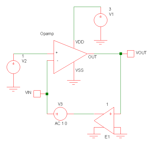
An improvement would be to add a unity gain voltage controlled voltage source (VCVS) in the feedback path to buffer the opamp output. The VCVS is the E source in SPICE:
Another option is to use the VCVS but with no resistors or capacitors and derive the open loop transfer function from the ratio of output to input voltage as show below:
In this case the gain is VOUT/VIN. A comparison of the results of the three methods using an IC opamp with very limited output drive capability is shown below:
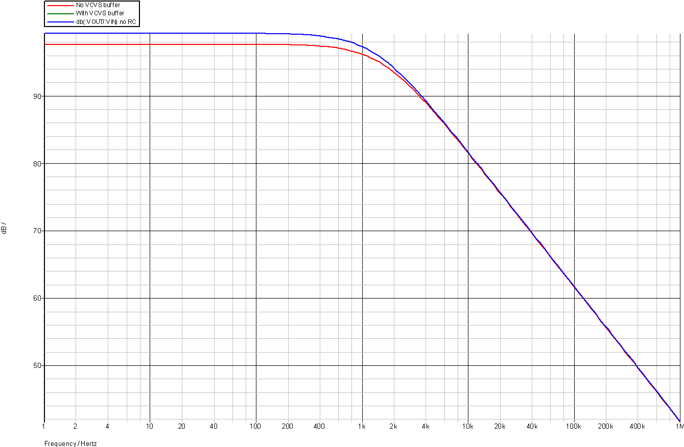
The results without the VCVS buffer show the effect of the limited opamp drive with a 10MΩ load. The results using the VCVS and the final method with no resistor/capacitor network are identical so the curves overlap.
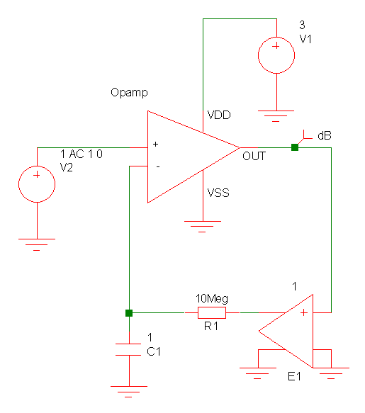
An alternative is to use two VCVS sources to totally isolate the feedback. This can be useful if the opamp has a finite input bias current and the DC levels will be affected. An example is given below where the opamp on the left has a 10mV output offset due to the 10MΩ feedback resistance.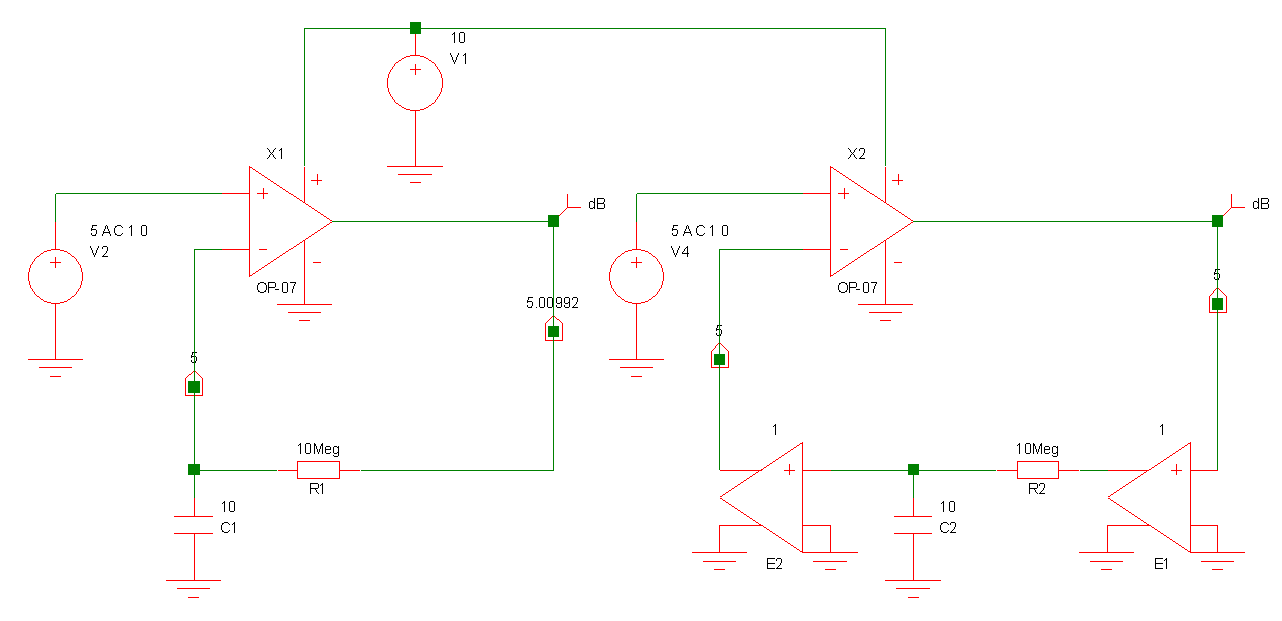
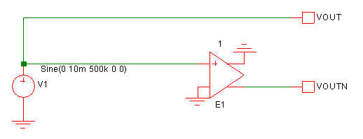
The VCVS has other uses such as if you want complementary signals. While this could be done with two separate voltage sources, if you want to alter the characteristics of one you then also have to edit the other. By connecting a VCVS with the output (or input) pins reversed you can have the two complementary signals – VOUT and VOUTN as shown below: